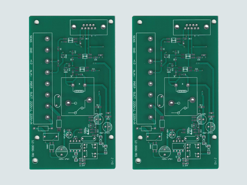
1, single-sided circuit board process blanking edge grinding → drilling → outer graphics → (full plate gold plating) → etching → inspection → screen printing resistance welding → (hot air leveling) → screen printing characters → shape processing → testing → inspection.
2, double-sided circuit board tin-spraying board process blanking edge grinding → drilling → copper sink thickening → outer graphics → tin plating, etching tin back → secondary drilling → inspection → silk screen welding resistance → gold-plated plug → hot air leveling → silk screen characters → shape processing → testing → inspection.
3, double-sided circuit board nickel plating gold technology process cutting edge grinding → drilling → copper thickening → outer graphics → nickel plating, gold film etching → secondary drilling → inspection → screen blocking welding → screen printing characters → shape processing → testing → inspection.
4, multilayer circuit board tin plate blanking edge grinding process flow to drill positioning hole, the inner graphics - lining etching - inspection - black - laminated to drilling to sink copper thickening, outer graphics, tin plating, etching annealing tin - secondary drilling - inspection - printing resistance welding - goldplating plug to hot air leveling, screen printing characters to form processing, testing and inspection.
5, multi-layer circuit board nickel plating gold plate process grinding edge → drilling positioning hole → inner graphics → inner etching → inspection → blackening → lamination → drilling → copper thickening → outer graphics → tin plating, etching tin back → secondary drilling → inspection → silk screen welding → chemical nickel plating → silk screen characters → shape processing → testing → inspection.


